Building An All-In-One 6502 Development Board
Some time ago, I made a simple, happy go lucky 6502 computer. I called it a minimal development board because that’s exactly what it was: the absolute bare minimum you could get away with. It was an invaluable tool for getting to grips with 6502 system design- and very little else as it turns out.
I always intended to outgrow that minimal development board, though perhaps not this quickly. What made me realize the ship was sinking was attempting to add a single IC to to the board. One new part. Just one.
Long story short, I ended up realizing just how inadequate my design was. You see, I have ambitions for the 6502. Ambitions that the minimal system board simply can’t achieve. Much as I don’t like to just give up on a project, no matter how flawed, I have to let that minimal board go. In it’s place I can build a board that ends up both simpler and more useful (and arguably just as broken!). Retrospectively, I ought to have done this from the beginning.
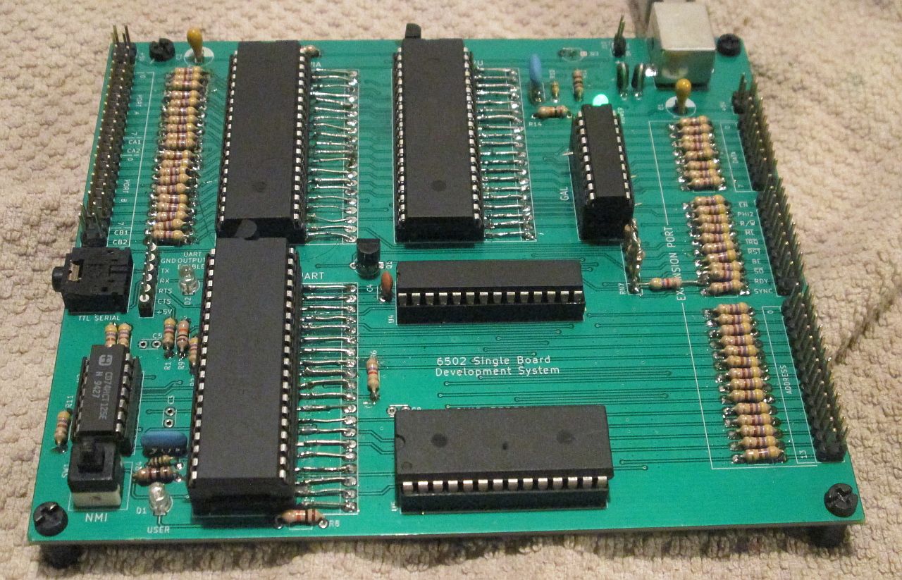
This new Single Board Development System is a one-stop shop for 6502 system design. It has a UART, a VIA, and 16KiB of external space you can plug all kinds of stuff into. It’s the sort of thing I wanted the minimal board to be. Lots of interesting projects require connecting the 6502 to various devices, which is effectively impossible to do on the minimalist board as it ended up. A real UART plus the parallel ports in the VIA are enough to prototype pretty much anything. Adding the expansion bus covers everything else.
While I was hoping this would be a nice, short, afternoon project there was so much wrong with my design that fixing it stretched over the better part of a week. Against all the odds, this troubled 6502 computer does work properly.
6502 SBDS Design
Part of the reason I’m ditching the old board is that it is vastly too complicated to work on. Not in the sense of too many features, but in the sense of too damn many wires.

Pictured: about seventy wires of all shapes and sizes.

A close-up to show you all just how impenetrable this rat’s nest is.
When you have a wire stack 20 layers deep, where even just moving a wire risks breaking it, where it’s trivial to wire things up incorrectly, and where there simply isn’t enough room to do anything, you must consider scrapping the whole project. Just sneaking a couple of new wires in is effectively impossible. By doing a from scratch redesign I can both build a better computer and make it more like the final system I’m envisioning.
Memory Map
In the minimal development board I used a 3:8 decoder to split the memory into eight 8KiB regions. This was a mistake. I had some design ideas that simply didn’t work out. Now I’m stuck with an underpowered board that can’t be reasonably upgraded to something useful.
For the new board I’m taking a more pragmatic approach that better reflects your average 6502 system:
| Address Range (Hexadecimal) | Size (KiB) | Description |
| E000-FFFF | 8 | EEPROM |
| D000-DFFF | 4 | 65C22 VIA |
| C000-CFFF | 4 | 16C550 UART |
| 8000-BFFF | 16 | Expansion port |
| 0000-7FFF | 32 | RAM |
While the unequal divisions require more logic overall, the use of GAL PLDs makes it a moot point.
This time around I’m dedicating a specific portion of the memory space to an expansion bus connector. Not having a dedicated expansion connector was a big design mistake. I need to use my development system to prototype hardware. Hardware is really hard to prototype when you can’t just plug it in.
RAM has been upgraded to 32KiB, in line with the most common SRAM chip you can get. ROM is stuck at 8KiB since the next biggest ROM is 32KiB.
I/O is changed from the UM245R, which turns out to be really hard to work with, to a TL16C550 UART and W65C22S VIA. These are dedicated LSI parts that make interfacing with other stuff pretty easy.
Part Count Reduction
In order to keep the cost of a PCB down, you need to minimize the total area. It’s much easier to do that when you have fewer parts to squeeze together.
Despite having more features than the minimalist board, the SBDS ends up being much smaller. Part of that is not having giant bundles of wire. Part of that is using a PLD to combine a bunch of small-scale ICs. But, most of the reduction comes from using dedicated I/O chips that don’t need much interface logic to begin with. The UM245R interface logic takes up about half of my prototyping board. Half.
Similarly the really crude reset circuit can be replaced by a dedicated power on reset part that fits in a TO-92 case. Some low-speed logic is replaced with NPN transistors. That removes almost all of the remaining support logic.
Power for these parts is, always has been, and always will be, +5V. Thinking about it, I realized I can just use USB power. That eliminates several parts.
All in all, the new board is only about half the size.
New Features
Pretty much every part got replaced, along with some added extras. Here’s a quick rundown of the new stuff:
W65C02 CPU-
My previous CPU was a Rockwell R65C02 rated at 2MHz. Good enough to learn about the 6502, but lacking in all kinds of features. Switching to the more modern W65C02 opens up a lot of possibilities.
Notably the W65C02 is rated up to 14MHz. In practice it is likely to go up to 20MHz. Hell yeah. Other nice features of the W65C02 are built-in bus buffers, a memory lock signal, and some handy new instructions.
TL16C550 UART-
Using the UM245R as the serial port turned out to be far more trouble than it was worth. Plenty of UART chips could be used, but I settled for the classic 16C550. Reasonably modern, lots of features, comes in a DIP package. Better than most of the alternatives, if nothing else.
I chose not to implement a true RS-232 interface. Nothing I have uses it. A simple low voltage serial interface will do just fine. I broke out the UART control pins in case I need them down the line.
W65C22S VIA-
Parallel ports are a common feature on computers of all types. Despite being a very simple concept, parallel ports require a lot of logic. More if you want features like bidirectional lines or handshaking.
Instead, the 65C22 Versatile Interface Adapter (VIA) implements a very flexible interface that is equivalent to at least thirty or so SSI/MSI logic parts. Included in the 65C22 are two 16 bit timers, an 8 bit shift register, and two 8 bit paralell ports with per-bit input/output configuration plus automatic handshake signals. It earns that versatile status.
Expansion PORT-
Any basic single board computer is enough to develop software for a CPU. But to develop hardware you need a way to plug random bits of equipment in. Almost every computer intended for “generic” applications has some kind of expansion bus.
I chose to set aside 16KiB of address space for external hardware. A simple pin-header interface is good enough to connect the raw CPU signals to prototype hardware. 16KiB of address space is more than enough for most hardware, and there are tricks to compress a large address space into 16KiB.
PROGRAMMABLE address AND DELAY LOGIC-
Using a GAL to simplify decoding logic is a no-brainer. One DIP-20 is doing the work of at least two or three DIP-14 parts. If I screw up the logic, well, I can just reprogram it.
Cranking up the CPU speed means some issues with timing. In particular, my EEPROM is very, very slow. (EEPROM always seems to be very, very slow). The 6502 has the RDY input that can be used to slow down the CPU for just this kind of purpose. Thinking ahead, I can use some of the unused pins on the GAL to generate the RDY signal when the ROM is accessed. Better, I can make it so different devices get different delays. All in one chip!
Other quality of life improvements-
A common problem when debugging is not being able to stop a rogue program without a total reset. By putting a switch on the 6502’s NMI line you can force any program to break into a debugger. Without a logic analyzer, this is probably the only way to pinpoint the exact address where your program is stuck. Without a detailed simulator (or ICE), it’s the only way to check the processor’s internal state. Adding the NMI switch is trivial.
Status LEDs are cool. Very useful for low level debugging. Unfortunately most LSI parts don’t break out interesting signals to hook LEDs to. I used the 16C550’s “out” pins to add some in for just this purpose. One shows the UART buffers are enabled, the other is independent.
6502 SBDS Schematics

Much cleaner than the ones for the minimalist development board, mostly as a result of finally figuring out how to use KiCad’s bus tools. They don’t really do anything, but they look pretty.
Just to be clear: there is no guarantee this schematic is error free. As we’ll see shortly, there was a lot wrong with this design. Most of that was the PCB itself, so schematics-wise, it shouldn’t be a big problem- but I don’t guarantee this schematic is error free.
6502 SBDS Construction
Having done the point-to-point wiring disaster that was the minimalist board, I decided to go straight to a PCB for this one.
Yes, this is expensive and inflexible. So was the point-to-point minimalist board. Sometimes the “cheap” option turns out to be way more trouble than it’s worth. While this board had some major errors, I could fix them relatively easily using simple patch wires. Debugging the minimalist board was much harder overall.
PCB Design
Thankfully, nothing about the PCB design needs special treatment. Just a standard, two side, simple rules PCB. The only extra was adding tons of redundant grounding vias. I want to push the CPU clock as far as possible- that means solid grounding is critical. You should do this anyways to keep noise under control.

It always feels good to have a proper PCB for your project, even if it turns out to be a real chore to fix up. Before reading further, try to spot the single most costly mistake.
Having learned a few hard lessons about leaving enough space between parts, I made sure to space things out generously. Very generously. Too generously, perhaps. I could probably take another inch off the board with a minor redesign.
Running signals off-board is asking for trouble in more ways than you can count. As a precaution, I added series resistors to all of the off-board signals. More advanced protection was rejected to lower part count.
Parts are cheaper in bulk, so I did the old trick of re-using the same handful of part values for everything I could get away with. The good news is the only part I need loads of- resistors- can be pretty vaguely specified. In practice the difference between 1K and, say, 470R or 2K2 is going to be minimal.
I used DIP footprints for all the “bulk” resistors. However it turns out these are way less common than I was expecting. Digikey only really had DIP-16’s in stock, which won’t work with this design. No matter. I was planning on using discrete resistors as a fallback anyways. There might be clearance issues if DIP packs are actually used.
Sockets were used for all the ICs because they are all expensive. I might need to use them in something else later on. Debugging is much easier when you have sockets, which turned out to be very helpful. Direct soldering would be fine, but keeping the ROM socketed is a good idea. Not every ROM can be programmed in circuit.
CPU speed is 10MHz. This is plenty fast enough for a small computer. I only need one wait state to use my ROM at this speed. I considered speeds up to 20MHz, but I would need 6 wait states. My RAM would also have trouble keeping up. Given 6502s perform memory access on almost every clock cycle, RAM delay would make the system slow down to about 10MHz anyways.
As for the TL16C550, I chose 4MHz. I already have a bunch of 4MHz resonators. At most I’ll need something like 19.2K baud. If I do need more, I can push this up to 16MHz.
Testing The SBDS
I went straight from schematic to PCB for this project. This may have been a mistake, as you’ll soon see. On the plus side, none of these problems are showstoppers like they were in my BLDC controller. Computers are slightly more forgiving than power inverters. Fewer things explode.
The good news is that none of them required a total redo. I have a bunch of barely working, hacked together parts, but I got it all working which is what really counts.
PCB Errata
Every single PCB I’ve ever designed seems to have at least one big mistake on it. Sadly the 6502 SBDS is not the exception. There are some real screw ups on this board!
By far the biggest, most embarrassing mistake is I somehow managed to use 1″ wide footprints for the DIP-40 parts. I cannot explain why I never caught this error, despite all the fretting over getting the development board just right. I just did, okay? The good news is that fixing this is relatively straightforward:

Make your own size jokes.

Sixty component leads and a lot of flux fumes later, I have “solved” this problem.
Of course, had I realized this before getting the boards made I could have shrunk the size down a little more. I’m probably a few dollars poorer over this mistake.
Back in the days when I tried to etch my own PCBs, I would sometimes print out a full size copy just to check if the parts were compatible with their footprints. This is a fantastic idea, and I’m not too sure why I stopped doing it. Probably because my preferred printer broke. Regardless, this is a good way to double check if everything is lined up properly. Would have caught the oversized footprints, at least.
Prior to the arrival of the SBDS, I tried putting the W65C02 in the minimal board. No particular reason, I just wanted to try it out. When it didn’t work, I got a little scared. I didn’t test the CPU when I first got it, and even a shitty CPU that’s old enough to be my dad is still pretty expensive. Oscilloscope probing revealed that I clearly didn’t RTFDS as well as I should have. One big, crippling difference between the R65C02 and the W65C02 is the latter does not implement any pull-up resistors on-chip. I knew that was true for RDY, but it turns out all input pins on the W65C02 lack this feature! I patched in a few new resistors on a couple lines I’d missed.

I didn’t have the proper type of resistor network, so I just built this monstrosity instead.
This does mean there was a schematic error where I didn’t put pull-up resistors on every single input- notably RDY. Originally I had RDY directly driven by the GAL; I changed over to an open collector line at the last moment. This would go on to have some unintended consequences.
I corrected the resistor oversight, but not in time for my PCB order. Now thoroughly paranoid, I checked the TL16C550 datasheet. No mention of pull-ups there either. Gotta slap some resistors over there, too.
Preliminary Test
Already this board is proving to be quite the problem. Even without the hacked together “solution” to improper footprints, I’m trying out some new ideas. Too many new ideas, perhaps. Clearly I need to double check some shaky assumptions.
Before going further, it would be prudent to check the absolute barebones basics of the SBDS wiring. This means digging out an old friend I didn’t really expect to see again: the NOPerator. You only need the CPU, address decoders, and clock for this test.

I can’t get all the hex values for addresses on one screen sadly. Ignore the RDY signal, it’s aliasing badly- but it is only turning on when the ROM is accessed.

A close up of RDY/CLK2 in blue/yellow respectively. RDY turns on at the left side, then produces a half-speed clock for ROM access.
I’m glad I did this, because getting the RDY logic right proved unusually tricky. Then I discovered that the open-collector RDY line simply didn’t work. At 10MHz there was hardly a blip on the oscilloscope. Even at 1MHz RDY was very unreliable. It topped out around 900KHz. Unacceptable!
Replacing the NPN transistor with a direct connection via 100R resistor (and reprogramming the GAL again) fixed the problem. I clearly need to come up with a better way to add multiple devices to RDY. Perhaps a simple AND gate would be good enough? Or a gate chain? Clock switching? Something to consider for later projects.
Test Program
With the PCB thoroughly mostly debugged, I can move on to testing the actual computer bits of the computer. There’s some ambiguity in how certain parts are supposed to behave. Using Modular Monitor is not possible at this stage, since I don’t really have an I/O stack written for the SBDS yet. Given I don’t yet know if the SBDS works that is not yet a task worth considering.
I came up with this short, sweet little program:
- Set the VIA timer to interrupt a known frequency
- Count interrupts to toggle the LEDs attached to the UART
- Repeat forever
Once again, in 6502 assembly:
.PC02
.include "VIA.A65"   ;Address constants for W65C22 VIA
.include "UART.A65"  ;Address constants for TL16C550 UART

INT_COUNT = $00      ;Slow blink counter

.CODE
INIT:
LDA #%11000000
STA VIA::ACR         ;Enable timer 1, with continuous interrupts and square wave output on PB7
LDA #%11000000
STA VIA::IER         ;Enable VIA interrupts
STZ INT_COUNT
LDA #$40
STA VIA::T1CL        ;Load lower half of counter
LDA #$9C
STA VIA::T1CH        ;Load upper half of counter, start counting automatically
LDA #$FF
STA VIA::DDRA        ;PORTA set to all outputs
LDA #$0C
STA UART::MCR        ;Initialize UART signals
CLI                  ;Interrupts ON

IDLE:                ;Loop forever, show interrupt count on VIA
LDA INT_COUNT
STA VIA::PORTA
BRA IDLE

IRQ:                ;Slow blink UART OUT signals
INC INT_COUNT       ;Count at 100Hz, blink at ~0.2Hz
BNE @EXIT
LDA UART::MCR
EOR #%00001100      ;Toggle OUT bits
STA UART::MCR
STZ INT_COUNT
@EXIT:
LDA VIA::T1CL       ;Clears VIA timer 1 interrupt flag
RTI


.segment "VECTORS"
.addr INIT
.addr INIT
.addr IRQ
This tiny test program covers basic operation of the CPU, ROM, RAM, VIA, and UART. It’s not an exhaustive test by any means, but if this little program doesn’t run I doubt anything else will.
Test Results
Well, this one took a while. First, I had issues with getting the VIA to count. I knew I could access the VIA since I could change the output lines. Counting proved fruitless despite multiple efforts. Turns out there is a very specific order of operations to turning the VIA timer on. You need to write to the high counter register, not the latch register. Okay, I haven’t really brought this up yet, but WDC’s datasheets are shit. Poorly worded with no examples. This is not the first time I’ve been burned by them. This blog helped me figure out the exact sequence to get my timer running.
Having sorted out the VIA, my attention turned to the UART. Nothing seemed to get it working, so I had to do some detailed probing. Eventually I stumbled upon the MR signal always being set- keeping the TL16C550 in perpetual reset. Turns out I had the pinout on the MCP101-450 wrong. Yet, this begged the question of why the rest of the circuit seemed to run just fine- ~RESET is derived directly from RESET. This was the fault of mistaking a PNP 2N3906 transistor over an NPN 2N3904. Happens all the time, I’m sure. Did I mention I’ve lost the magnifying glass I use to read part numbers?
Having sorted the reset stuff out, the UART still didn’t work. I did a variety of tests, including completely rewiring the control signals. For a while I figured I was improperly setting up the control signals- some kind of race condition or timing violation. I ended up using the rest of the GAL outputs to try and correct this. No change. Turns out the bug was much, much, sillier.
Take a look at the pinout for the TL16C550. Notice it has complimentary read and write signals. Contrary to what I was expecting, you don’t need to assert them simultaneously. You’re supposed to wire the unused input to the disasserted state- they’re ORed together, not ANDed. Unintuitive, since normally you wire unused but related control signals to be true. Consider the CS signals on the very same TL16C550- they must all be true to get access to the chip.
Anyways, I had wired the UART so it was always trying to read and write simultaneously. Thankfully it appears Texas Instruments (or whoever originally designed this UART) seem to have added some lockout logic to minimize the problems with this illegal state. Nothing was harmed. Two jumper wires fixed the problem.

Patching out the errant control signals was mercifully simple. Even if the little grabbers keep falling off. A more permanent solution is being developed.

At this point, I seem to have finally crushed the last of the serious bugs. There are still occasional problems with sudden lockup, likely due to problems with my socket “adapters” or perhaps a few unsoldered connections. Those I can live with, for a while at least.
And so, after several days of intense debugging, I finally had a working computer:

Finishing Up
Sometimes you learn how to do something right by first doing it wrong. My minimalist board was a brave attempt that didn’t really work. SBDS fixes up all the practical problems while adding new features. If I knew then what I know now, I would have done things this way from the start. But, I didn’t. So I had to learn the hard way. That’s just the way it goes sometimes.
I hate ordering PCBs because I know, I just know, I’ve managed to screw them up somehow. How can you consistently fail to choose the wrong footprints? I keep doing it, despite additional caution. Really not a good track record I’m building here. On the plus side, I am fast becoming an expert in PCB modification.
Originally I wanted to also release the PCB design files. After running into all the PCB errors, I quickly realized the SBDS is not ready for a full release. Perhaps sometime in the future, when I redo the board.
I used a GAL to handle address decoding because it simplifies the circuit. It wouldn’t be that hard to eliminate it. Both the 16C550 and 65C22 have multiple select inputs that could handle most of the addressing logic. Unfortunately this logic alone can’t completely cover the address decoding. The GAL at least allows for more flexibility in the circuit design. Putting the delay logic in the GAL is also significantly simpler than using discrete logic.
A design decision I now regret is not adding a reset button, instead relying on NMI to do the same thing. In practice, the W65C02 has the STP instruction that requires a full reset to get out of. I’m pretty sure I already ran into issue during my debugging sessions. Trigger STP by mistake, and you have to either power cycle the board or short RST to ground somehow. Other than that, the VIA and UART don’t always play nice with a software-driven reset.
There was only one 10MHz resonator in my parts collection. It was salvaged from… something I have long forgotten. I ended up breaking it completely during testing, so I slapped on a 4MHz resonator instead. 4MHz is still twice as fast compared to the minimal board, though I expect to replace it when I can get more parts. With RDY directly driven from the GAL, this should still work okay.
Many minor simplifications were rolled into this design. Most of them are pretty trivial, so I didn’t talk about them. Let’s just say I’m far more comfortable with the 6502’s control signals now.
Much of this design was based on parts I already had to hand. That’s why the MCP101-450D is there. I bought them a long time ago, found out they output the wrong polarity signal, and they were looking for work ever since. I feel there are better ways to handle the reset signal, though they all involve buying new parts. Something that can handle a manual pushbutton reset, ideally.
My experience with the 6502 thus far has not been that pleasant. Much of that is inherent to the 6502 itself, which is a fussy old CISC accumulator machine with some frustrating limitations. The rest was simply getting the circuitry together. Computers require a lot of connections. You’d be surprised just how long a computer can run with a bad connection.
I have a few 6502 projects that will need to use the minimal development board in the interim- porting them over to the SBDS will be more trouble than they’re worth. You’ll see some of them soon enough. Once I get Modular Monitor ported over, I expect to switch all development to the new system. I can do much more interesting stuff on the SBDS.
Have a question? Comment? Insight? Post below!