A Classic Power Supply Project With Ample Utility.
Every electrical device needs a power supply. Usually we just pick some “black box” supply from a supplier, but when testing you need something more flexible. To that end, every respectable electronics laboratory has an adjustable constant voltage/constant current power supply. With a simple twist of a dial, the output envelope can be tightly controlled.
You can of course just buy a CC/CV power supply. It’s standard equipment, after all. This both robs you of an interesting project and potentially leaves you with a shitty, burned out supply. Cheap power supplies are usually badly made with a long list of problems. At least when my design explodes into surprise pyrotechnics I can look at my bad design decisions and make something less incendiary.
For this project, I wanted something that could power up small electronic projects. Turns out you don’t need too much for that. 20V/2A is plenty, though there’s no reason this couldn’t be extended to the standard 30V/3A and beyond. Heat is ultimately the limiting factor.
Overview
Your typical bench supply is a linear type. A linear power supply is effectively an infinitely variable impedance. You put a load on the output terminals and the impedance dynamically changes to keep the voltage/current constant. Excess energy is disposed of as heat.
A simple analogy here is holding down the accelerator of a car and regulating speed by braking as required to slow down (DO NOT DO THIS. You have been warned!). This is extremely inefficient, and the efficiency drops the greater the difference between input and output. What it lacks in efficiency is made up for in simplicity. Where power loss is low, this is a tradeoff usually worth making.
The other big advantages of linear regulation are low noise and high stability. Both very useful for a laboratory supply.
Chances are you’re familiar with the 78xx or LM317 “three terminal” regulators already. They work on similar principles but lack the features of a proper laboratory type power supply. Adding those features requires building the regulator circuitry from scratch.
How Not to Design a Linear Power Supply

You would not believe just how many times this particular schematic pops up with only minor variations.
All of them are rubbish and should be immediately discarded.
Before going further, I have to take moment to briefly explain how not to build a good power supply. Spend a few minutes searching and you’ll find plenty of dodgy designs.
In particular, many designs power the regulator electronics directly off of the input source. Taking power this way has enough disadvantages to scare off anyone with a modicum of prior knowledge:
- Delicate electronics are exposed directly to the entire input voltage. Most op-amps only tolerate 30 to 40 volts. Some chips tolerate even less, sometimes below 5 volts.
- Interfacing the amplifiers to the pass transistor is difficult. If the pass transistor is lifted off ground, like in many bad designs, this voltage must be added to the turn on voltage. Usually this is the entire output range.
- Alternatively, the regulator transistor is inserted between load and ground, rather than source and load. This simplifies the control circuit, but adds the exciting design flaw of allowing a short to ground that bypasses the regulator.
- It can be difficult to get the output to turn all the way off. Generally op-amps need to pull negative to completely turn off a load. This means an extra negative supply is required on top of the already high-voltage being applied to the regulator.
Put it all together, and the op-amp has to tolerate an extra 10-20 volts over the nominal output range- up to 50V for a 30V output range. Good luck finding an op-amp that can handle that. Better luck getting it cheap. There’s also a bunch of extra support circuitry just to make the op-amp work.
A much better solution is to split the supply into two circuits. One is the power circuit, which handles the high voltage/high current stuff. The other is the regulator circuit, which just powers the op-amp and associated parts. The only expense is an isolated low-voltage supply.
By isolating the regulator supply from the output supply, all of the problems with the one-supply system are solved. Op-amp voltage can be reasonably low, the ground can be anywhere we want to put it, and the op-amp supply can be split around ground to get a negative voltage. You’d be a fool not to do it this way.
The other more subtle reason why these designs suck has to do with loop compensation. Chaining multiple op-amps into each other is a great way to run into stability and/or transient response problems.
Much like splitting the power supply into two sections, current and voltage are split into separate control systems. They act independently, taking over control when conditions mandate. Loops can be optimized/stabilized without troubling the other one.
Building the Bench Supply
This project is several years in the making. Despite getting a functional prototype built fairly quickly, the project languished. Sometimes you just can’t find the motivation to finish something up, you know?
Part of that hesitancy is that a power supply is a fairly complex undertaking, even if it is relatively simple conceptually. There are a few traps for the inexperienced scattered along the way. I generally don’t like it when expensive stuff explodes, so I spent a lot of time making sure things went as planned. There were still some major cock-ups (including one small explosion) but I got through to the end mostly intact.
Circuit Design
It took a while to find a good circuit. I ended up scraping together the design basics from multiple sources- particularly service schematics of old equipment. Much SPICE simulation followed. I feel pretty confident in the final circuit.
I’m a bit divided on whether to call the whole power supply circuit complicated or not. It looks pretty intricate, but it’s nothing you won’t see in an introductory electronics course. Just basic op amp and transistor circuits. Parts were chosen primarily for availability and cost.

Because only one op-amp should control the output at any time, blocking diodes are added. That means they can only sink current, so drive current is provided by a current source. Therefore the default state is on.
During startup that causes a race condition between the control circuit and the output voltage. This results in the infamous “turn-on spike” poorly designed supplies make. Adding the delay circuit keeps the output off until things stabilize.
Incidentally, this is another thing those bad designs never even acknowledge. Curiously, most designers don’t seem to acknowledge the cause is a race condition, even when they acknowledge the spike. Maybe my background in digital design makes that easier to see?
There’s a little more to talk about that’s not part of the main circuit. Here’s the schematics:

AC power is input via an “entry module”. This is an all-in-one component with connector, fuse, switch, and sometimes a filter. Easier and safer than trying to build it yourself.
Power for the main output and control circuit is provided by 24 and 12.6 VAC transformers. After rectification these provide 33.9 and 17.8 VDC respectively. Actual measurements are quite a bit more, because transformers are wound to compensate for their own internal resistance. At low currents I get 40V or more out of the main transformer. This caused a brief panic over my 35V input capacitor. After a bit of frantic research, I concluded a 13% overvoltage is probably okay. Probably. Nothing’s exploded yet. Yet.
Control is provided by the coarse and fine potentiometers. I decided against multi-turn types because they are expensive and potentially ambiguous. General life advice, don’t design stuff where “maximum” looks identical to “minimum”. Just trust me on this. I added an extra 3k3 resistor between the potentiometers to give me a little more flexibility. They aren’t critical, just a convenience for my particular setup.
Circuit Construction
I made several test circuits, starting with a breadboard prototype. Breadboard circuits aren’t meant to last, so I have nothing to show. At this point I discovered the original design I wanted to use was shit, so I went searching around for a design that worked. This is when I started to appreciate just how many power supply schematics are terrible.
When I got the new design working properly, I moved up to a protoboard. I got some good practical experience with the circuit. It still exists; presumably it still works. Because protoboards aren’t fitted for power components I had to resort to a lot of hackery to make it work.

You can see a rather different set of components than in the given schematics. Most of them involved working around a non-split regulator supply.
My prototype was okay, but had a few problems of it’s own. At this point I was designing around switching supply modules as pre-regulators. Eventually I threw those out in favor of old-fashioned transformers with rectifiers.
Changing to transformers drastically changed the rest of the circuit. I could cut out a lot of newly redundant parts. On the downside, I had to add in some components to handle the AC input. I guess it balanced out in the end.
I finalized the basic circuit, and started working on a PCB. It was this that had me fretting away a couple of years. Getting a board done isn’t that cheap. I also had to wait a month for it to arrive or pay more for fast shipping. So, I kept putting it off.
During that time, I kept re-designing the board. Slowly, it began to resemble the final product. What kept me tweaking it was the case; I built part of the case before ordering the final boards. Squeezing everything inside required some Tetris-ing, and I was never really happy with it. I made a couple of layout revisions, but there’s only so much that can be done.
Eventually I said to hell with it, and ordered the PC boards. When they arrived, I quickly set about soldering one up. A few years of pedantic “looking busy” became a few hours of “get it done”.

You know it’s just so nice to have a real PCB for once.
Despite having some complex PCB designs under my belt, I continue to screw up all the time. While mostly correct, there were still some significant design errors.
In particular that giant input capacitor did not match the footprint I chose- the leads are too fat. I had to drill out the holes, then scrape off the solder resist to get a connection. Works okay for now.
I didn’t consider the size of the connectors for the low-voltage signals. They cover up the silkscreen telling you what the signal is. Voltage and amperage controls are just far enough apart to squeeze their connectors in. I should have shuffled things around to put a little more space between them, or perhaps flip them to face different directions.
When I did my preliminary tests, maximum output gave a pathetic 0.2V. Eventually I traced this back to the voltage feedback resistors being transposed. Turns out this was not an assembly error but a schematic error. I duly updated the schematic.
I neglected to provide a bleed resistor. After a few terrifying probe-induced sparks, I soldered one directly to the input capacitor terminals. That sparking caused a trace to blow so I patched in some wire-wrap wire to fix it. Nothing else was damaged.
Beyond that, there weren’t any problems with the board itself, just some hamfisted modification work. I replaced the original TIP3055 with a TIP140, but couldn’t quite get the old solder out of the holes. Excessive pressure was applied. I ended up with buckled leads. Rather than solder up a new board I just decided to live with it.

It might not look too bad from this angle, but the leftmost lead on the power transistor has a pretty big fold in it.
Check out that burnt flux too- my soldering iron was broken and overheating at this time.
While plugging everything together, I broke a tab off of the smaller transformer. I put it back in place with some epoxy putty.

You can see the little gray blob on the transformer holding in the broken tab.
Apologies for the not-great image quality. Turns out it’s really hard to get good photos of this thing.
Case Construction
From the very beginning, I decided the case had to allow for the entire circuit- PC board, transformers, meters, everything- to be removed as one unit. I settled on a U-shaped aluminum sheet as a base. This makes the chassis, front, and back panel in one unit.
I added aluminum angle bars across the top to improve rigidity. As it turns out, this greatly simplified adding the cover.

I don’t have any pictures without the electronics mounted. You can still see the important bits clearly. Well, clearly enough.
To complete the case, I made a complimentary U out of 1/2″ plywood. I just screwed the pieces together. Much like the metal part of the case, I added a little wood bar across the bottom front to stiffen it. This also keeps the bottom of the aluminum chassis off the table, so I can put exposed screw-heads down there.

You can see the top sheet cut away at the front and back. I had to do that to fit the little lip the sheet metal makes at each end. On the plus side this significantly improves how securely the inner chassis is held.
I finished up by gluing some wood trim over the front to hide the edges. The back is left open to allow the chassis to be slid out. Two extra strips glued to the bottom to act as feet.
Connecting the two case halves was simplified by putting those bars in. Without them, there aren’t a lot of places to put the mounting screws. I poked some holes into both halves, threaded the aluminum, and added some cone-head screws. Simple and neat.

I just about got the screws flush with the top of the case. Impressive considering I didn’t have a countersink bit at the time.
Getting the two halves to fit is a little tricky due to… let’s call them “manufacturing tolerances”. Much better sounding than poor build quality. Once the mounting holes are roughly aligned, the screws pull the case together snugly, poor tolerances or not.
Linear power supplies need serious heatsinking. I riveted three U-shaped aluminum fin assemblies to the back. These ended up being pretty crude, but they make a significant impact on cooling.

A better choice would have been a lot of L-shaped fins. I chose against this on the grounds drilling all those holes was a lot of work. Perhaps it wasn’t.
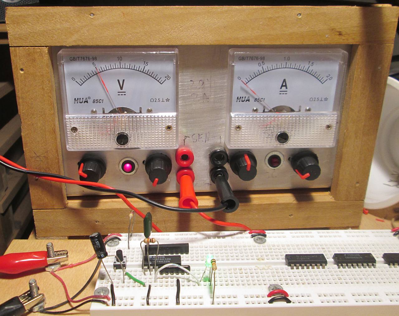
On the front is what you’d expect. Meters, connectors, and controls.

One of these days I’ll put real labels on my projects.
These particular meters have an odd mounting footprint. You need a sort of “Mickey Mouse” shaped hole to fit them. I ended up tweaking them a little too much. They’re loose enough to go crooked after a while. Annoying.
Connectors are standard banana jacks. I chose the socket type over the binding post type for cost reasons. Thinking about it, I probably couldn’t realistically fit binding posts in that tiny little area. You can’t exactly undo holes in sheet metal, so I’m stuck with what I have. I tried to mount them 3/4″ apart. They’re close enough for a flexible double-plug.
I got some reasonably cheap knobs from Adafruit. Better than anything I was planning to do. Coarse control is on the left, fine to the right. CC/CV LEDs are fitted in between.
My only real complaint with this design (other than the aforementioned “manufacturing tolerances”) is that I neglected to mount the bottom of the chassis to the outer case. When you go to plug in a test lead it pushes the panel back. Maybe I’ll fix that someday.
Testing
With the entire power supply finished, it’s time to do proper testing. You definitely need an oscilloscope for this. I cannot think of a way to check transient response without one. Thermal testing requires a thermometer, preferably a thermocouple.
Transient Performance
First up is transient testing. I grabbed a MOSFET and plugged it into the power supply, an oscilloscope, and a signal generator. I set the power supply up for maximum voltage and current. Then I set the signal generator to provide a low frequency square wave to turn the MOSFET on and off, repeatedly shorting the output.
This setup simulates the worst possible scenario: hard switching between the extremes of both control loops. If the power supply can handle this, it can handle just about anything. Same for any other system.

Hooking in that MOSFET was a bit tricky. Eh, I’ve had to do more with less.

Output response in yellow, MOSFET drive in blue.
Also, I just realized the USB drive text is there. It’s not covering up anything important, so I’m going to let it go.
I think my oscilloscope can calculate the relevant numbers automatically. I couldn’t make it work, so I had to do it manually. With measured values this is trivial.
Percent overshoot is the highest value reached before the signal settles down compared to the desired output. I got about 5%. Good enough.
Based on this overshoot, the damping factor is 0.69. TL082s are compensated to about this factor. I suspect that compensation is doing most of the work.
Settling time is the time it takes the signal to settle down, typically to <5%. A whopping 280us in my case. I’m a bit mystified by why it takes so long. Twiddling the current knob shows it’s the current limiter kicking in. What confuses me is this is about 5x longer than it should take given the output capacitance. It won’t be a huge issue, so I guess I’ll leave it at that.
Despite doing nothing much to stabilize or optimize the loops, they work just fine. Loop compensation is complicated, so this is fine by me. Typically these power supplies are stabilized by adding more capacitance to the output- at the expense of transient response.
I am a little worried by the ringing at the switchover point. Putting 100nF on the end of the cable effectively cures it, while putting it directly on the output terminals has minimal effect. That would imply it’s from the inductance of the cable, not the power supply itself.
Thermal Performance
Second up is the thermal testing. This is complicated by the fact that I tried to swap the silicone thermal pad I was using with a better interface. That was a bad idea. Silicone has thickness to fill in small gaps. My replacement did not. I had to throw out a lot of calculations because of that little snafu.
Measuring the heatsink performance is simple. Put a constant load on the output (e.g. Simple Load, though a short circuit can work just fine if you’re careful), measure the heatsink temperature as close to the power source as possible. Wait until the measurement plateaus. Repeat for a few different power settings.
Keep in mind, the relevant voltage is not the output voltage, but the difference between the unregulated input voltage and the output voltage. The power supply is working hardest when the load is a short circuit; i.e. load voltage is zero. I made all my tests by shorting the output and adjusting the current. I used 33.9V as the input voltage. A few volts here and there won’t really matter much.
Crunching the numbers I got a combined thermal resistance of about 2C/W; equivalent to a sustained power dissipation of about 50-ish watts. That’s not quite enough to use the full output current at low voltages (I’d need 1.5C/W or less for that). I consider that acceptable- most uses of a power supply are less strenuous. A professional power supply usually makes the same assumption anyways.
Finishing Up
Much like Simple Load before it, this is a project too long in the making. I spent a lot of time wringing my nerves over nothing. Having since built it, it has all but replaced the modified ATX power supply I was using before. By now it’s kind of hard to remember how I limped along without a proper power supply for so many years. Sometimes you just don’t know what you want until you’ve got it.
Nothing is perfect; neither is this power supply. The front panel is cramped, crooked, and feels a bit too flimsy. Sadly I can’t fix that without making a new case. Which I don’t want to. So I won’t.
I’ll need to touch up the wooden parts of the case once it gets warm enough to put them outside. I’ll do any extra case work then. Otherwise the case is completely satisfactory.
What keeps tripping me up with PCB design is making sure the finished footprints are properly matched to the components. I got it better this time around, though that input capacitor is embarrassing. Another PCB design tip is to put dedicated test points down. Much easier than shorting out high power connections with a badly placed probe.
While getting the final pictures for this article, the voltage control stopped working. I had to open the case to get the last images, so I took the opportunity to fix it. Bending the potentiometer seems to have fixed it. I suspect the little phenolic board is warped. I’ll probably have to do a more serious repair in the near future.
Despite my motivation behind Simple Load being testing this project, Simple Load ended up not really being all that useful. Don’t worry, Simple Load has proven it’s worth on other projects. Chances are you’ll hear about some of them if you stick around.
Overall, I’m right chuffed with how this whole project finished up. Useful product, useful experience, no big failures, nothing left to do. Time to focus on something else for a while.
Have a question? Comment? Insight? Post below!