Fixing Up A Boost Converter Design
Not that long ago, I designed, built, and tested a simple boost converter circuit. I even wrote all about it! Despite some clear shortcomings, I concluded it was “good enough”. Engineers, such as we are, are pretty good at “good enough”. You never should work any harder than you need to. Perfectionism is the killer of so many good ideas. Just let go. Try not to think too much about what could have been.
Unfortunately engineers, such as we are, are pretty bad at leaving “good enough” alone. There were some obvious flaws in the circuit that I could not help but try to fix. Even before I was done writing that article I was hard at work designing and testing an improved circuit. By adding just three extra components the boost converter circuit was improved to the point where it actually kind of surprised me.
By every measurable metric this new circuit is better across the board. Efficiency went up. Output current went up. Reliability went up. Sometimes a couple of minor tweaks really can make all the difference!
The Discrete Boost Converter Circuit As It Stands
For those of you catching up, I wrote up a whole article about building and testing this particular circuit. Read it over here. Here’s the schematic I ended up with, for reference:

The primary thing I found was that while acceptable, there were significant improvements that could be had. Some I discussed in the previous article, some I chose not to. Here’s the short list of things I noticed needed improvement:
- Quiescent current was very high, a few mA worth.
- Efficiency was okay, but just barely acceptable.
- Output regulation was poor, with worrying spikes.
- My prototype was badly constructed and kept falling apart.
Except for the last point these can all be addressed by tweaking the circuit a little bit. The last point is a construction problem which can also be addressed.
Discrete Boost Converter Redesign
Whenever you’re building this kind of project, even as a throwaway one, you’re always trying to minimize effort. More often turns out to be less in the engineering world. More parts, less space to put them. More connections, less reliability. More time spent designing, less time spent building, even less time spent using. I chose to carefully add on to my boost converter circuit, testing each change thoroughly. If a modification didn’t help much, I didn’t keep it. After quite a bit of iteration, I arrived at this circuit:

Three extra components that are well worth adding!
All the changes target the feedback network. While it still works the same way overall, there are two modifications that dramatically change how well the circuit works.
First, the addition of a second NPN transistor allows the current through Q1 to be cut, rather than wastefully shunting Q3’s drive current to ground. This dropped the quiescent current so low I can’t actually measure it anymore. I was surprised by just how effective this was. Well worth the addition of two components.
Second, the emitter of Q3 now goes through a 0.1R resistor. Voltage feedback is grounded through this resistor too. This feeds information about the current going through Q3 (and the inductor) through to Q4. Adding even a little current feedback improves the circuit behavior. It makes the switching cycle shorter and more predictable, both of which are a problem with self-oscillating boost converters. Efficiency improves, and the exact value of the inductor is less important. Well worth the cost of an extra component.
Note that I have eliminated the snubber. It didn’t really do much. From what I’ve managed to gather you can’t realistically add the snubber until after you get the circuit working anyways. Two parts I can (temporarily) eliminate. Net result: one part added. I call that an engineering victory.
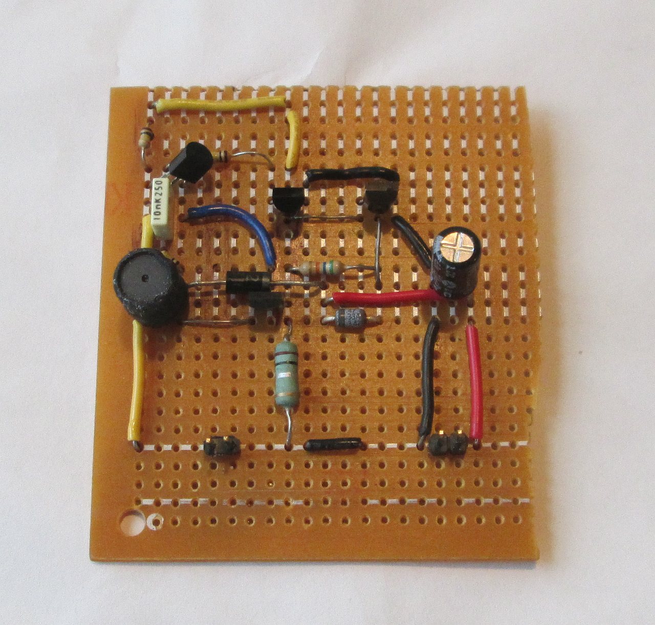
Building A Prototype Discrete Boost Converter
Up until now I’ve been breadboarding this boost converter circuit. Breadboards and power circuits just don’t get along that well. While I can get the circuit working, there are still issues with high resistance connections, components getting pulled out, that sort of thing. Because the breadboard gives me such a headache, I chose to build a proper prototype on some perfboard scraps. Perfboard also isn’t great for power circuits, but it’s much better than a breadboard.


PCB design may seem complicated, but it’s a hell of a lot smoother than this. Note a rough soldering job with a couple of hasty fixes.
You wouldn’t think cramming the circuit together would be that challenging. You unfortunately would be wrong. I had to make a few compromises on how everything is laid out. The problem is less one of circuit complexity, more one of protoboard shittiness. I’m unwilling to spare a larger board, nor buy a new one. So I just had to knuckle down and figure it out.
I’m not entirely happy with the prototype design. Even given my constraints I think I could do better. But for a temporary project I just don’t think it’s worth it.
Testing The Improved Discrete Boost Converter
Testing uses the same setup using Simple Load and my bench supply. My goals remain the same: 70% efficiency, 4.5 to 5.5 volts output, operable between 3 to 4.2 volts.

At least this circuit doesn’t fall apart when you try to probe it. Note the breadboard with the test circuit still half-built.
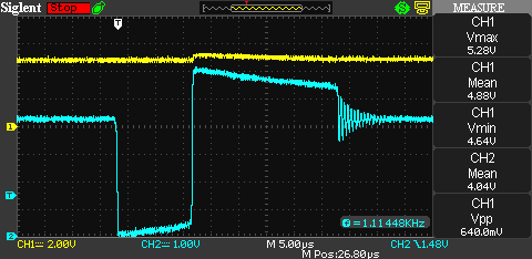
Oscilloscope trace is about what you’d expect. Without a snubber that output rings like a bell.
| Input Voltage | Input Current @150mA Load | Output Voltage | Efficiency @150mA Load | Maximum Output Current |
|---|---|---|---|---|
| 3.0V | 340mA | 4.72V | 69% | 240mA |
| 3.5V | 275mA | 4.72V | 73% | 330mA |
| 4.0V | 220mA | 4.76V | 81% | 480mA |
Well, would you look at that! This new circuit is behaving a lot better all-around. I attribute most of the improvement to eliminating unreliable connections in the power loop. Beyond that, the operating frequency is more stable due to current feedback. These figures are almost bang-on what I’m getting from SPICE.
| Input Voltage | Quiescent Current (Estimated) |
|---|---|
| 3.0V | 320uA |
| 3.5V | 280uA |
| 4.0V | 300uA |
Quiescent current is now so low it’s effectively unmeasureable. I tried several techniques but I just can’t get decent readings. These values are all taken from SPICE. By the by, simulating such a low power circuit puts SPICE in a real bad place where the calculations completely break down. I had to add a 100uA load just to get it to behave properly.
I did try to calculate the quiescent current with what information I had. My estimate is a 125uS pulse of 250mA average with a repetition rate around 1.5 seconds. Assuming I manged to wrangle the numbers properly, that equates to something like 20uA. I’ll take the higher numbers for worst-case design calculations. Either way, it’s at least an order of magnitude better than before.
Finishing Up
Good engineers tend to be minimalists. We strive to trim off as much fat as possible. Adding parts sometimes feels like failure. Like you couldn’t figure out how to do it properly and hacked it together with the electronic equivalent of duct tape. Engineers also tend to be very results driven, and you really can’t argue with these results. Three new components make for an objectively better circuit. I think this is a perfect example where extra complexity is justified.
Obviously this boost converter circuit won’t be as stable, simple, or cheap as a proper boost converter IC. However I’m actually kind of surprised by how competitive it is. While I couldn’t recommend building your own boost converter for most practical power supply projects, there’s definitely a couple of niche applications for a circuit like this.
Reduction in quiescent current is by far the most valuable improvement. Compared to the MC34063, this particular circuit operates at about 1/5th to 1/8th of the quiescent current. Given the ease by which I managed this feat, I really don’t know why the MC34063 has quiescent current that high. You could probably use this circuit in an “always on” project powered from a battery- as long as the circuitry being powered also has low quiescent current.
Despite being better, this boost converter circuit still has a few problematic quirks. ESR in the output capacitor has a pretty dramatic effect. Too high, you get some serious output spikes. Too low, the circuit doesn’t always oscillate. The exact value of this capacitor is also troublesome. Self-oscillating DC-DC converters need some ripple on the output to work properly. No way out but to thoroughly test the prototype.
Out of sheer curiosity I put a magnet on the power inductor. This caused the operating frequency to rise dramatically with no noticeable change in efficiency or output power. Static magnetic fields effectively pre-saturate the inductor, so this behavior isn’t surprising. Normally you want to avoid a switching inductor saturating. Here it’s not so much of a problem. A low saturation current is actually advantageous because it forces the operating frequency higher, out of audio range.
2025 is fast proving to be a pretty brutal year for us all. In just five months the entire global order has collapsed, fundamental civil rights have been abruptly cancelled, and economic depression looms large. If this is bad, I’m frightened by the worse things to come.
While the world crumbles around us, I’ll do what I can to keep these projects going. I may have to change what I plan to do dramatically, and I probably can’t keep to a reasonable posting schedule anymore, but given what’s going on that’s just how it’s going to have to be.